Sunday, 5 February 2017

Adjustable HV Power Supply for Stompbox


This SMPS can be powered with low input voltage, from 5 VDC to 15 VDC and provided adjustable Output Voltage: + 92 Vdc to +340 Vdc.

Can be used too, as power supply, for the Xenon Lamp, Nixie tube Clock, VFD display, Magic Eye, Neon, and too many others electronics circuits who need HV power supply to work. Is great to use with many models of Nixie tube. It can drive 6 Nixie tubes, in multiplex mode, from 180 to 200V. Powered with low voltage from 5VDC to 15 VDC. With this SMPS you can power 250V @ current of 7.5mA! *In all case above, important note, DC and AC filters must be improved, if is desired reducing present HF frequency noises at output! Another fact, informed before, the RF energy is irradiated as magnetic and electric field, shielded assembly could be necessary!


Thursday, 12 January 2017

1-to-2 KM LONG RANGE FM TRANSMITTER


Here i am going to explain you a building of simple fm transmitter using a two transistor . I will try to explain as possible as i can. lets starts with the components required.

Transistor
Q1= BC547
Q2=2N2219

Capacitors
C1 & C2 =4.7uF(electrolytic)
C3,C4 &C7 = 100nF( ceramic 104)
C6 = 4.7 pF (ceramic )
C5= 10-30 pF (Variable capacitor or also known as  TRIMMER )

 Resistors
R1= 47K
R2= 220K
R3=4.7K
R4 & R5 =10k
R6= 100 ohm

 INDUCTOR
L1=  8 turns of 22 Gauge copper wire around a simple ball pen.( I will upload a photo of it for more idea)

 POWER SUPPLY
Battery (Power Supply) = 12-9 V DC (Always use battery and avoid adepter so i will    
                                                                        reduce  noise in transmission )

  HOW FM CIRCUIT WORK ?  :

The circuit is basically a radio frequency (RF) oscillator that operates around 100 MHz. Audio from audio jack is fed into the audio amplifier stage built around the first transistor. Output from the collector is fed into the base of the second transistor where it modulates the resonant frequency of the tank circuit (the 8 turn coil and the trimcap) by varying the junction capacitance of the transistor. Junction capacitance is a function of the potential difference applied to the base of the transistor. The tank circuit is connected in a Colpitts oscillator circuit. It works on the principal of COLPITTS Oscillator.

 ANTENNA IS MUST IN THE CIRCUIT:

A impudence matching ANTENNA is must required in the circuit,without Antenna circuit will never works .Generally we uses a telescopic antenna . which through the waves in the atmosphere .

2 to 5 Km Range Long Range Transmitter Circuit


The proposed long range transmitter circuit really is very steady, harmonic free design which you can use with standard fm frequencies between 88 and 108 MHz.

This will likely encompass 5km spectrum (long range). It includes an extremely consistent oscillator for the reason that you employ LM7809 stabilizer that is a 9V stabilized power source for T1 transistor and for frequency realignment that may be reached by means of the 10K linear potentiometer. The output strength of this long range rf transmitter is approximately 1W however may be more significant should you use transistors like KT920A, BLY8, 2SC1970, 2SC1971…

Transistor T1 is employed as an oscillator stage to present a small power steady frequency. To fine-tune the freq. apply the 10k linear potentiometer this way: should you moderate, in the direction of ground, the freq. would probably decrease but when you fine-tune it in direction of + it would climb. Essentially the potentiometer is needed just as a flexible power source for the a pair of BB139 varicap diodes. Both of these diodes function as a changeable capacitor whilst you regulate the pot. By tweaking the diode capacitance the L1 + diodes circuit renders a resonance circuit for T1. Feel free to employ transistors similar to BF199, BF214 however be careful not to use BCs. At this point you don’t receive yet the long range fm wireless transmitter due to the fact that the electric power is fairly reduced, a maximum of 0.5 mW.

The proposed transmitter circuit works in the following manner:

Always encase the oscillator stage in a metal guard to avoid parasite frequencies destabilizing the oscillating stage.

Transistors T2 and T3 functions as a buffer stage, T2 as a voltage amplifier and T3 as a current amp. This buffer stage is vital for freq stabilization simply because is a tampon circuit between the oscillator and the preamp and final amplifier. It happens to be renowned that bad transmitter layouts normally change freq. whenever you alter the finalized stage. Using this T2, T3 stage this won’t occur again!

T4 is a preamplifier stage and is employed as a voltage power rf amplifier which enables it to produce adequate power to the ending T5 transistor stage. As is demonstrated T4 carries a capacitor trimmer in its collector, this is definitely accustomed to render a resonance circuit designed to drive T4 to promote more advantageous situations and do away with those undesirable harmonics. L2 and L3 coils has to be at 90 degrees perspective one to another, this is to prevent frequency and parasite coupling.

The concluding stage of the long range rf transmitter is equipped with any rf power transistor containing no less than one watt production power. Utilize transistors like 2N3866, 2N3553, KT920A, 2N3375, 2SC1970 or 2SC1971 should you wish to produce a professional fm transmitter with ample power to take care of an extended spectrum zone. Should you use 2N2219 you will definitely get a maximum of 400mW. Make use of an effective heatsink for the T5 transistor because it becomes slightly warm. Make use of a reliable 12V/1Amp balanced supply of power.

How to Set-up the Transmitter

Begin by building the oscillator stage, solder a tiny wire to T1 10pF capacitor out and hearing a fm radio, tweak the 10k pot until it is possible to “hear” a blank disturbances or maybe if you connect an music base you could listen to the melodies. With a 70cm cord it is possible to take care of a 2 – 3 meter region simply with the oscillator stage.

Next carry on and construct the remaining of the rf transmitter, utilize correct shielding as suggested in the above explanation. As soon as you have completed the transmitter design, hook up the antenna or more effectively a 50 or 75 Ω resistive load and make use of this as a rf probe, feel free to use 1N4148 diode in place of the probe diode.

Fine-tune yet again the 10k pot to favored freq. thereafter go to T4 stage and scale down the initial collector trimmer for highest voltage signal on the multimeter. After that carry on with the subsequent trimmer and so forth. After that get back on the very first trimmer and readjust yet again until you receive the maximum voltage on the multimeter. For one watt rf power you could possibly ascertain a twelve to sixteen Voltage. The method is P (in watt) is equivalent to U2 / Z, wherein Z is 150 for 75Ω resistor or 100 for 50Ω resistor, nevertheless one should keep in mind that the proper rf power is lesser.

After those modification, in case things are heading nicely hook up the antenna, keep on employing the rf probe, readjust once more all of the the trimmers right from T3. Guarantee you don’t have harmonics, verify the TV and radio set to determine if there exists fluctuations on the band. Verify this in an alternative area, a long way away from the fm transmitter or antenna.

The unit is all set up to be used for exchanging music, talks, chats across the suggested range and bands.

Long Range Transmitter Circuit - 2  to 5 Km Range


All Inductors are air cored


L1 = 5 wounds / 23 SWG / 4mm silvered copper
L2 = 6 wounds / 21 SWG / 6mm enamelled copper
L3 = 3 wounds / 19 SWG / 7mm silvered copper
L4 = 6 wounds / 19 SWG / 6mm enamelled copper
L5 = 4 wounds / 19 SWG / 7mm silvered copper

T1 = T2 = T3 = T4 = BF199
T5 = 2N3866 for 1Watt / 2SC1971, BLY81,or 2N3553 for 1.5 to 2W power.


3 km ranged FM transmitter circuit

FM transmitters have been used all over the world for communication. The simplicity of building a FM circuit made it so popular among other modulation techniques. Today i have come up with FM transmitter circuit which has a range of about 3 Km approximately. The circuit diagram was pretty wide and i cannot fit it into this webpage. Click on it to see large resolution image. Let’s get into the working part of this circuit.


WORKING OF FM TRANSMITTER:
There was a lot of components and parts in this circuit so i will keep the explanation simple as possible. This is a good quality FM transmitter with a stable frequency brought by the modified oscillator, which is actually two oscillators built around Q2 and Q3 working at around 50MHz in anti-phase. The output is taken at the two collectors, where the frequencies of the two oscillators combine to form a 100MHz signal. This will provide a greater stability than normal single ended oscillators.


The modulation is done via the dual varicap D1/D2 and the variable capacitor C8. By changing the reverse bias voltage on the varicap (according to an input signal) you essentially change their capacitance thus the resonance frequency of the tank circuit. This leads to frequency modulation of the input signal virtually. The output of the oscillator/modulator stage is fed to a class A driver stage built using the transistor Q4. The output signal is further strengthened by feeding in to a  class C power amplifier built around Q5.

Now feed the output signal from Class C  to low pass filters made of series of Capacitors and Inductors. This is done to achieve lowest harmonics spurs at the output before feeding it to the antenna. I have added an indicator LED D3 which shows that you’re transmitting and everything is working fine. If the LED doesn’t light up then something is wrong with the schematic. The problem usually occurs in the oscillator part (just for a hint). Also I managed to remove almost all variable capacitors but the one for the tuning, because the original schematic had a lot more variable capacitors and it’s hard to tweak them all.

RANGE OF FM CIRCUIT:
The power of output signal in this FM circuit is 2.5W . At 2.5W FM signal is capable of covering 5 – 7 Km distance with good line of sight. And in best case scenario it might even reach 10km approximately. So i believe it will be fair to say that this circuit will cover 3 Km range even under semi optimum or worst external conditions.

This circuit was  designed for European FM receiver systems although it’ll work in America as well, I’m not really sure if the audio quality will stay the same. That comes from the fact that I’ve used a 50us preemphasis which is the European standard and USA works with 75us preemphasis.

PCB TIPS: 
When building this circuit, there are few PCB considerations which you have to follow. It’s very important to use a ground plane instead of a ground rail when wiring the system. This increases the ground area and stability. You can also build a balun just before the antenna feed line by coaxing 3 or 4 turns of the coaxial cable with a length of 21 inches. As a result this will create a resonant trap for electrical fields flowing on the cable’s outer shell, and prevent making it to part of the antenna, which is undesirable.

NOTE:
Never start the transmitter without a load.
If you haven’t connected the antenna just put a dummy load resistor of 50ohm at 2W (carbon, not wire wound) and test your circuit.


Wednesday, 11 January 2017

50W FM Radio Station

It can cover  3 to 8KM radius in ideal environment . It include: one 50W FM transmitter, one antenna, one 20M coaxial cable, one  mixer, two microphones, two BOP covers, two headphones, two speakers, two microphone stands, one aduio processor.


How to build FM Telephone Bug

Here is a simple transmitter that when connected to a phone line, will transmit anything on that line (execpt the dial tone) to any FM radio. The frequency can be tuned from 88 to about 94Mhz and the range is about 200 feet. It is extremely easy to build and is therefore a good, useful beginner project.
Circuit diagram
Parts
R1 180 Ohm 1/4 W Resistor
R2 12K 1/4 W Resistor
C1 330pF Capacitor
C2 12pF Capacitor
C3 471pF Capacitor
C4 22pF Capacitor
Q1 2SA933 Transistor
D1, D2, D3, D4 1SS119 Silicon Diode
D5 Red LED
S1 SPDT Switch
L1 Tuning Coil
MISC Wire, Circuit Board
Notes
1. L1 is 7 turns of 22 AWG wire wound on a 9/64 drill bit. You may need to experiment with the number of turns.
2. By stretching and compressing the coils of L1, you can change the frequency of the transmitter. The min frequency is about 88 Mhz, while the max frequency is around 94 Mhz.
3. The green wire from the phone line goes to IN1. The red wire from the phone line goes to IN2. The green wire from OUT1 goes to the phone(s), as well as the red wire from OUT2.
4. The antenna is a piece of thin (22 AWG) wire about 5 inches long.
5. All capacitors are rated for 250V or greater.
6. The transmitter is powered by the phone line and is on only when the phone is in use. S1 can be used to turn the transmitter off if it is not needed.
7. If you have problems with the LED burning out, then add a 300 ohm 1/4W resistor in series with it.

How to build 3W FM Transmitter

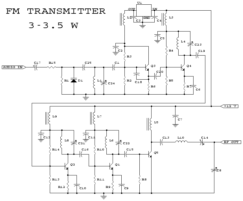
his is the schematic for an FM transmitter with 3 to 3.5 W output power that can be used between 90 and 110 MHz. Although the stability isn't so bad, a PLL can be used on this circuit.
This is a circuit that I've build a few years ago for a friend, who used it in combination with the BLY88 amplifier to obtain 20 W output power. From the notes that I made at the original schematic, it worked fine with a SWR of 1 : 1.05 (quite normal at my place with my antenna).

Circuit diagram


Parts:
R1,R4,R14,R15 10K 1/4W Resistor
R2,R3 22K 1/4W Resistor
R5,R13 3.9K 1/4W Resistor
R6,R11 680 Ohm 1/4W Resistor
R7 150 Ohm 1/4W Resistor
R8,R12 100 Ohm 1/4W Resistor
R9 68 Ohm 1/4W Resistor
R10 6.8K 1/4W Resistor
C1 4.7pF Ceramic Disc Capacitor
C2,C3,C4,C5,C7,C11,C12 100nF Ceramic Disc Capacitor
C6,C9,C10 10nF Ceramic Disc Capacitor
C8,C14 60pF Trimmer Capacitor
C13 82pF Ceramic Disc Capacitor
C15 27pF Ceramic Disc Capacitor
C16 22pF Ceramic Disc Capacitor
C17 10uF 25V Electrolytic Capacitor
C18 33pF Ceramic Disc Capacitor
C19 18pF Ceramic Disc Capacitor
C20 12pF Ceramic Disc Capacitor
C21,C22,C23,C24 40pF Trimmer Capacitor
C25 5pF Ceramic Disc Capacitor
L1 5 WDG, Dia 6 mm, 1 mm CuAg, Space 1 mm
L2,L3,L5,L7,L9 6-hole Ferroxcube Wide band HF Choke (5 WDG)
L4,L6,L8 1.5 WDG, Dia 6 mm, 1 mm CuAg, Space 1 mm
L10 8 WDG, Dia 5 mm, 1 mm CuAg, Space 1 mm
D1 BB405 or BB102 or equal (most varicaps with C = 2-20 pF [approx.] will do)
Q1 2N3866
Q2,Q4 2N2219A
Q3 BF115
Q5 2N3553
U1 7810 Regulator
MIC Electret Microphone
MISC PC Board, Wire For Antenna, Heatsinks

Notes:
1. Email Rae XL Tkacik with questions, comments, etc.
2. The circuit has been tested on a normal RF-testing breadboard (with one side copper). Make some connections between the two sides. Build the transmitter in a RF-proof casing, use good connectors and cable, make a shielding between the different stages, and be aware of all the other RF rules of building.
3. Q1 and Q5 should be cooled with a heat sink. The case-pin of Q4 should be grounded.
4. C24 is for the frequency adjustment. The other trimmers must be adjusted to maximum output power with minimum SWR and input current.
5. Local laws in some states, provinces or countries may prohibit the operation of this transmitter. Check with the local authorities.